Diamond NV Centers (Solid-State Defects)
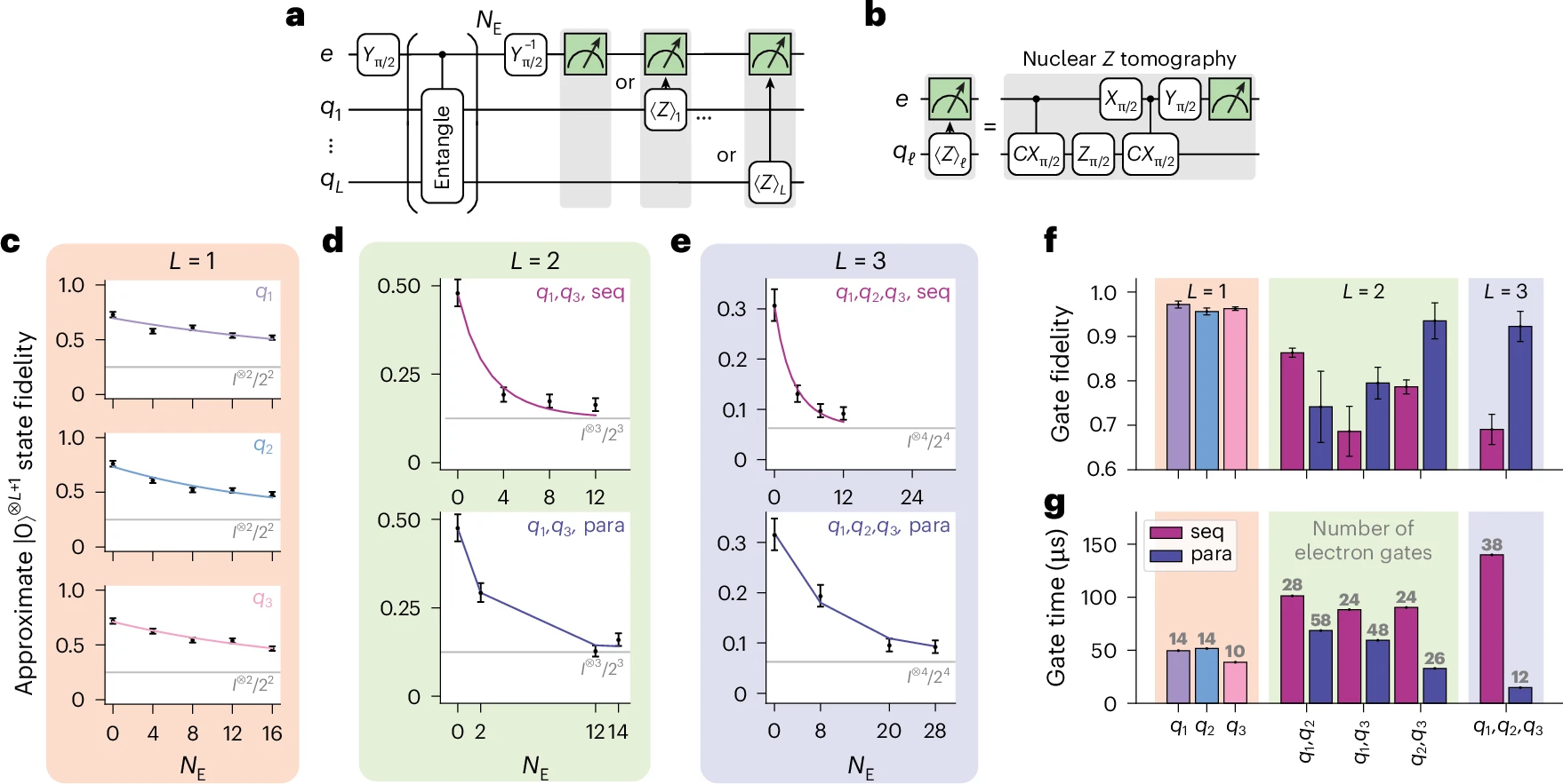
A research team at the University of Pennsylvania achieved parallelized many-body quantum entanglement on a room-temperature diamond quantum register using a single microwave gate operation, successfully preparing a four-qubit GHZ (maximally entangled multi-particle) state in 14.8 microseconds [4].
In terms of technical significance, generating multi-qubit entangled states in solid-state NV (nitrogen-vacancy) diamond systems was previously constrained by serial microwave pulse operations between the electron spin and surrounding nuclear spins; creating four-qubit entanglement typically required sequential multi-gate pulses with total runtimes routinely exceeding 150 microseconds. By employing global single-gate driving to realize parallel entanglement, this approach compressed state preparation time from approximately 150 microseconds down to 14.8 microseconds—a tenfold acceleration in many-body entanglement generation—while markedly suppressing decoherence noise accumulation during the operation [4].
Benchmarked against the State-of-the-Art (SOTA):
① Extent of progress: In room-temperature solid-state quantum systems requiring zero cryogenic refrigeration, generating a four-qubit GHZ state in 14.8 microseconds sets a new benchmark for parallel multi-qubit manipulation on room-temperature chips. However, benchmarked against cryogenic superconducting SOTA—where superconducting two-qubit gate times typically span 20 to 100 nanoseconds (e.g., Google’s Willow chip)—and trapped-ion routes—where two-qubit gate times range between 10 and 500 microseconds (e.g., Quantinuum Helios achieving a two-qubit gate fidelity of 99.921%)—the operational speed of this room-temperature diamond gate reaches the regime of slower trapped-ion gates, yet remains two to three orders of magnitude slower than superconducting gates. In terms of scale, 4 physical qubits remains in a very nascent laboratory prototype stage compared to 1,180 physical qubits in neutral-atom platforms (Atom Computing) or 105 physical qubits in superconducting platforms.
② Remaining gaps: This pathway still lacks critical components for practical fault tolerance: severe spin decoherence caused by lattice phonon scattering at room temperature limits coherence times from sustaining deep quantum circuits, and closed-loop surface code (2D topological quantum error-correcting code) cycles have not yet been demonstrated; furthermore, the absence of an end-to-end loss budget for high-fidelity inter-chip optical interconnects impedes engineering scaling from a single 4-qubit node to multi-node arrays in a quantum network.
In terms of landscape impact, this breakthrough provides physical-layer validation for eliminating reliance on liquid-helium dilution refrigerators and engineering lightweight, vehicular, or portable quantum computing and quantum sensing modules, offering a scalable architectural template for future quantum technologies [4].
Superconducting & Semiconductor Manufacturing Interfaces
GlobalFoundries officially finalized a $375 million award agreement under the U.S. CHIPS and Science Act to expand its quantum technology solutions manufacturing facility in Malta, New York. The site leverages its 22FDX (22nm FD-SOI) process to mass-produce cryogenic CMOS (cryo-CMOS) control and readout chips along with advanced heterogeneous quantum packaging components [6].
In terms of technical significance, superconducting and spin quantum processors have long been throttled by the "wiring bottleneck"—each physical qubit operating in the millikelvin regime typically requires two dedicated coaxial cables running to room-temperature server racks, making thermal isolation and volumetric scaling unsustainable as systems scale beyond thousands of qubits. By tailoring low-temperature transistor behavior on its mature 22nm process, GlobalFoundries has developed digital and RF control integrated circuits capable of stable operation at 4 Kelvin, aggregating thousands of discrete RF cables into a minimal set of high-speed serial digital buses [6].
Benchmarked against SOTA: In terms of advancement, this manufacturing line transitions on-chip control and advanced packaging for superconducting and silicon-spin modalities onto 300mm commercial wafer mass-production lines, aligning with commercial wafer-scale integration standards set by Intel and Diraq. However, comprehensive high-precision cryogenic noise models (PDKs) for transistor devices down to the millikelvin regime remain incomplete, and microwave insertion losses during flip-chip hybrid integration between superconducting chips and silicon-based CMOS control dies have yet to be fully resolved.
In terms of landscape impact, this funding secures the first dedicated commercial wafer foundry capacity in the United States serving quantum hardware developers, reducing North American quantum startups' reliance on Asian packaging and foundry supply chains. Starting in 2027, it is anticipated to drive down rack-level integration costs for dozens of superconducting and silicon-spin hardware companies [6].