Oct 15, 2026 – Oct 16 · Daily Brief

Google Cuts Hardware Overhead for Practical Quantum Computers by Over Thirtyfold

54 items · 13 sourcesPDFThis issue's roundup is free
02Hardware

Hardware Frontier

Superconducting Chips and Wafer Fabrication

Commercial quantum foundry Anderon announced the release of the first superconducting quantum PDK (Process Design Kit, a standardized component library regulating chip fabrication) on its 300 mm wafer line at the Albany NanoTech Complex, backed by $2 billion in funding to provide a variety of superconducting wafer foundry services[18][39]. In terms of progress, this achievement advances superconducting chip fabrication from custom laboratory runs or 200 mm pilot batches to semiconductor-standard 300 mm mass-production wafer substrates, establishing standardized commercial foundry rules for the superconducting roadmap for the first time; against hardware SOTA (state of the art) baselines, current leading superconducting systems such as IBM Heron (156 qubits) and Google Willow (105 qubits) still rely on proprietary fabrication lines and dedicated processes—while Anderon matches advanced CMOS processes in wafer diameter, public statistical data on microwave component parameter uniformity and yield remains unavailable. Gaps remaining: The core bottleneck of superconducting quantum chips lies in $T_1$ (energy relaxation lifetime, the dissipation time of quantum state energy) being constrained by TLS (two-level system defect) fluctuations at dielectric interfaces; in the baseline, Willow's average $T_1$ of ~100 microseconds still experiences 2- to 3-fold temporal fluctuations, and 300 mm large-format wafers still face severe process ramp-up challenges in large-area Josephson junction uniformity and TLS defect density control. Landscape impact: This directly benefits fabless superconducting quantum hardware startups by reducing tape-out trial-and-error costs and disrupts the traditional capital-heavy vertically integrated model with a foundry division of labor, projected to drive superconducting quantum computing toward a specialized division between fabless design houses and dedicated pure-play foundries within the next 2 to 3 years.

A research team utilized baseband flux pulses to achieve ultra-fast, high-fidelity control of superconducting qubit states, compressing single state-switching time to 10 nanoseconds[27]. In terms of progress, this result pushes control pulses directly into the ultra-fast 10 ns regime; against hardware SOTA baselines, single-qubit gate durations in current commercial superconducting systems typically range from 10 to 30 nanoseconds, while two-qubit gate durations fall within the 20 to 100 nanosecond window (IBM Heron and Google Willow), and a 10 ns switching speed approaches the physical frontier of superconducting Josephson junction dynamic control. Gaps remaining: Baseband flux pulses can easily induce population leakage and high-frequency transient distortions inside superconducting chips; baseline single-qubit gate fidelity thresholds are no less than 99.95%, and this experiment has not yet disclosed full-chip composite crosstalk and gate fidelity data under parallel operation on multi-qubit chips, leaving an engineering gap before meeting fault-tolerant control requirements. Landscape impact: This will force superconducting microwave control boards to undergo architectural upgrades toward higher-sampling-rate baseband generation over the next 1 to 2 years.

Trapped Ions and Neutral Atoms

ETH Zurich, in collaboration with startup ZuriQ, successfully implemented two-qubit logic gate operations in a Penning trap (an electromagnetic particle trap confining ions via magnetic and electrostatic fields) using microwave control instead of traditional lasers, achieving control speeds comparable to electron spin qubits[29]. In terms of progress, this work demonstrates that all-electromagnetic microwave-addressed control can be achieved in high-magnetic-field Penning traps without laser driving; against hardware SOTA baselines, the record for trapped-ion two-qubit gate fidelity is 99.99% (single-pair measurement), with the highest commercial all-to-all pair fidelity being 99.921% in Quantinuum Helios; while this achievement marks a crucial step in eliminating laser phase noise, a full suite of benchmark gate fidelity data has not yet been published. Gaps remaining: In large-scale 2D ion crystals within Penning traps, microwave gradient fields decay extremely rapidly and can easily induce electromagnetic crosstalk among adjacent ions; furthermore, the inherent ion-transport overhead and limited cycle repetition rate (cyclic operation frequency per second) bottlenecks in trapped-ion architectures have not yet been effectively resolved from an engineering standpoint in such compact high-field structures. Landscape impact: If microwave schemes mature, they are projected to simplify trapped-ion systems from complex, bulky laser optical setups into semiconductor chip-scale packaging within 3 to 5 years.

Molecular Spins and Solid-State Materials

NVision, pivoting from hyperpolarized MRI, unveiled its PIQC (Photonic Integrated Quantum Chip) molecular computing architecture, which deposits synthetic organic molecules with optically addressable spin states onto silicon photonic chips to construct quantum hardware[19]. In terms of progress, this approach attempts to combine the long coherence times of solid-state molecular spins with the high-density optical interconnects of silicon photonics; against hardware SOTA baselines, photonic systems (such as PsiQuantum's chips fabricated on GlobalFoundries' 300 mm wafer line, with two-qubit fusion fidelity of 99.22% ± 0.12% and detection efficiency $\ge$ 95%) employ all-optical encoding, whereas the molecular spins utilized by NVision remain at the materials prototype stage. Gaps remaining: Deterministic precision positioning and alignment of molecular spins on silicon photonic wafer surfaces, mitigation of inhomogeneous spectral broadening, and end-to-end loss budget tables for photonic interfaces are entirely absent; overall maturity metrics lag behind mainstream superconducting and trapped-ion roadmaps by more than two generations. Landscape impact: As an early-stage, high-risk exploratory path, it poses no substantive threat to the existing superconducting and trapped-ion commercial landscape in the near-term 5-year window.

Researchers developed a novel high-frequency testing methodology that enables rapid, continuous characterization and readout of qubit properties in 2D van der Waals materials for next-generation quantum computing[6]. In terms of progress, this scheme compresses the readout cycle of 2D-material quantum-dot devices from milliseconds down to the microsecond scale; against hardware SOTA baselines, the spin quantum-dot SOTA (e.g., atomic-precision donor qubits achieving two-qubit gate fidelity of 99.99%, with sampled fidelities exceeding 99% on 300 mm production wafers) has advanced to multi-qubit logic gates, whereas 2D material systems remain in the physical characterization phase of single quantum dots, lagging commercial targets in coherence time and gate fidelity by more than two generations. Gaps remaining: Interlayer contact resistance and interfacial charge noise control in 2D materials remain unbreached, lacking a stable, error-correction-grade single- and two-qubit control baseline. Landscape impact: Provides 2D novel materials laboratories with faster high-throughput screening tools, shortening the trial-and-error cycle for fundamental devices.

03Algorithms

Algorithms and Software

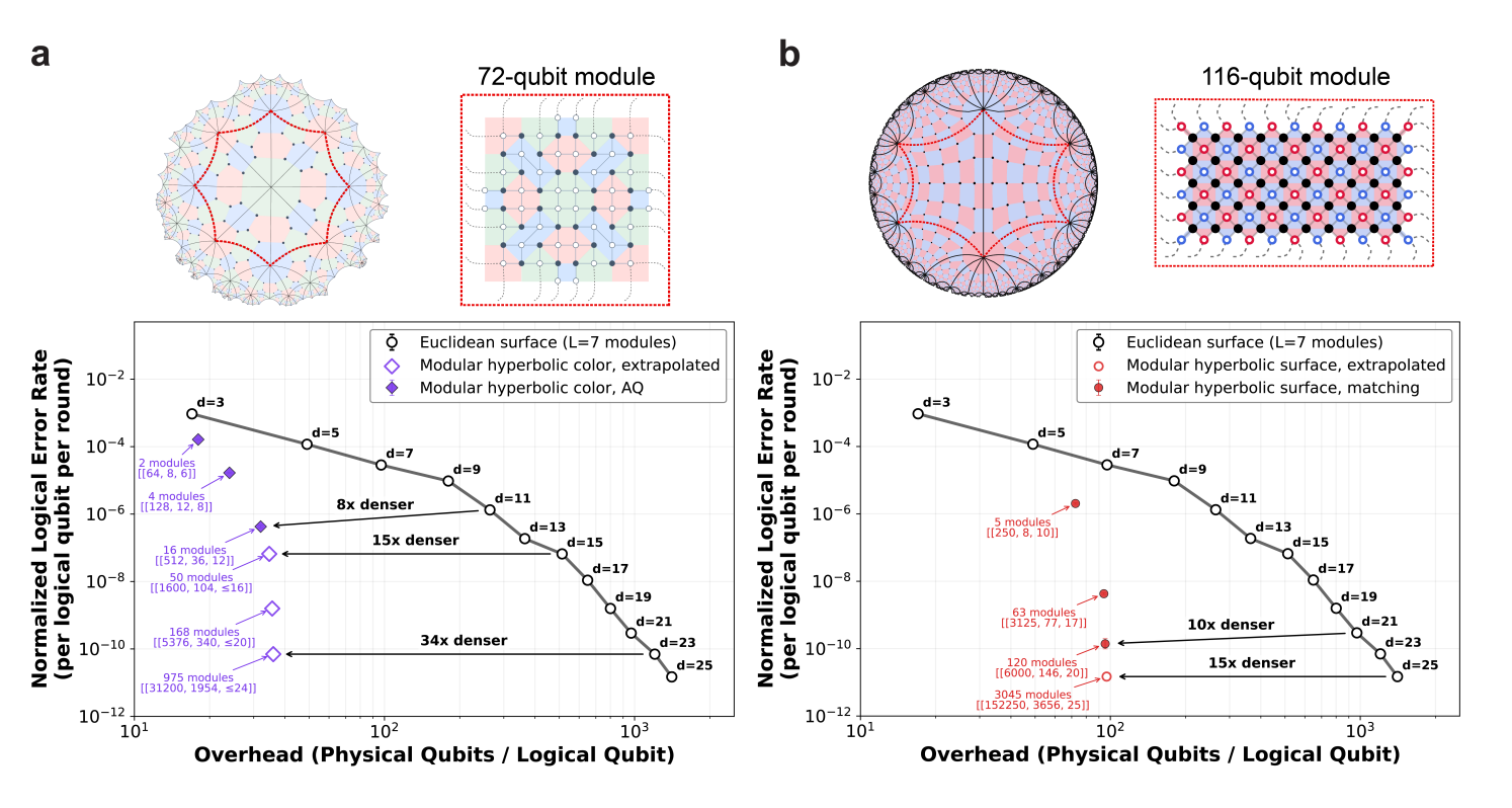
The Google Quantum AI team, in collaboration with DeepMind and MIT, posted new research on a preprint server proposing a modular hyperbolic code architecture that reduces the physical qubit overhead required for error correction by more than 30 times compared to standard 2D surface codes (the current mainstream planar topological error-correcting code)[14]. Technically, the encoding rate of traditional 2D surface codes decays sharply toward zero as code distance grows, typically requiring physical-to-logical qubit ratios of 100:1 or even 1000:1 for fault-tolerant computation (e.g., Google Willow reaches a 105:1 physical-to-logical ratio under surface codes, whereas Quantinuum's concatenated codes achieve a best of 2:1); hyperbolic codes exploit non-Euclidean geometric topological connectivity to achieve a non-zero asymptotic encoding rate while preserving local modular connectivity, realizing over 30x physical qubit redundancy compression in a modular architecture for the first time[14]. In terms of landscape impact, fault-tolerant full-stack system developers across both superconducting and neutral-atom modalities stand to benefit directly; if realized with chip-scale integration, this architecture could lower the design threshold for fault-tolerant machines from hundreds of thousands of physical qubits down to the order of thousands, accelerating the commercialization timeline of fault tolerance by 3 to 5 years.

A team led by Hengyun Zhou at MIT, in collaboration with Harvard researchers, designed a high-density, compact QEC (quantum error correction) code achieving an encoding rate of more than one logical qubit per two physical qubits (an encoding ratio better than 1:2)[22]. Technically, this design directly outperforms the best physical-to-logical encoding ratio in previous publicly reported global hardware SOTA baselines (Quantinuum's 2:1 based on concatenated codes, with 48 logical qubits mapped to 98 physical qubits, compared to QuEra at ~4.7:1 and Atom Computing at ~49:1); in terms of theoretical compactness, it crosses the unit overhead barrier, proving that high-rate error-correcting codes do not require massive stacking of physical qubits[22]. In terms of landscape impact, this compels the error-correction theory community to pivot comprehensively toward ultra-compact LDPC (low-density parity-check) code designs, favoring hardware architectures with non-local, flexible connectivity, such as neutral atoms and trapped ions.

IBM Research developed an automated agentic workshop based on open-weight algorithmic models for fully autonomous exploration and design of specialized quantum error correction decoding chip architectures, achieving hardware execution speedups of up to 204x while reducing agent inference computing overhead by 11.5x[16]. Technically, this overcomes the real-time decoding deadline in superconducting fault-tolerant systems where decoder latency must remain strictly below qubit coherence times (superconducting decoherence is typically on the microsecond scale, requiring millions of syndrome measurement data points to be processed in real time); by replacing manual hardware description language (HDL) development with automated agentic space search, it establishes a rapid, low-cost iteration pipeline for dedicated decoding ASIC (Application-Specific Integrated Circuit) chips[16]. In terms of landscape impact, this clears a critical decoder engineering bottleneck for fault-tolerant computing, signaling that with the anticipated rollout of kiloqubit-scale chips by 2027, error-correction decoders will fully transition into an era of dedicated on-chip hardware.

Sweden-based FirstQFM announced that, combining its patented pulse-control foundation model with Quantum Machines' OPX hardware and QUA control stack on an NVIDIA computing platform, it reduced single-qubit gate duration by 33% without degrading gate fidelity on QuantWare's 21-qubit Contralto-D21 superconducting quantum processor[17]. Technically, cutting single-qubit operation time by a third without degrading superconducting gate fidelity is directly equivalent to increasing the number of executable coherent operations within the hardware coherence time by nearly 50%, while embedding pulse-optimization algorithms deeply into low-level real-time control firmware[17]. In terms of landscape impact, this provides full-stack superconducting system integrators and the control-and-readout board supply chain with a plug-and-play upgrade path at the pure firmware level, instantly enhancing the circuit depth of near-term noisy quantum chips.

Quantum software startup SoftQuantus introduced its QCOS quantum operating system, demonstrating hydrogen molecule simulations based on VQE (Variational Quantum Eigensolver, a hybrid algorithm for approximating molecular ground-state energies) and incorporating cryptographic auditability mechanisms to achieve verifiable quantum computation execution[11][12]. Technically, this addresses the compliance pain point in hybrid quantum-classical computing executed in the cloud where output results cannot be safeguarded against tampering and forgery through conventional cryptographic means[11][12]. In terms of landscape impact, this directly serves pharmaceutical and chemical materials giants with stringent compliance requirements regarding computational intellectual property and data privacy.

04Industry

Industry and Ecosystem

The German Federal Ministry of the Interior (BMI), Federal Ministry for Digital and Modernization (BMDS), and Federal Office for Information Security (BSI) jointly issued a national PQC (Post-Quantum Cryptography, next-generation encryption algorithms designed to resist quantum cracking) migration guideline aligned with the EU post-quantum roadmap, establishing a three-stage migration timetable: mandatory implementation of hybrid encryption mechanisms, replacement of high-risk systems by 2030, and complete migration across all systems by 2035[15][40]. Commercially, this signals that Europe's largest economy has officially upgraded post-quantum cryptography from an industry initiative into a mandatory statutory compliance threshold; hybrid cryptographic mechanisms (running classical and quantum-resistant algorithms in parallel) were designated as the sole legitimate transition technology path during the migration period[15][40]. In terms of landscape impact, global financial institutions, telecom operators, critical information infrastructure contractors, and security chipmakers face rigorous regulatory assessments, which is expected to unlock billions of euros in spending over the next 5 years for cryptographic asset discovery/inventory audits and hardware security module (HSM) replacements.

Following its disclosure on October 16 Beijing time of unaudited revenue reaching $16.3 million for the first three quarters of 2026 (a 65% year-over-year increase), Nasdaq-listed SEALSQ announced that it currently holds $465 million in capital reserves dedicated to accelerating mass production and R&D for its semiconductor chips, PKI (Public Key Infrastructure), and post-quantum security hardware[21]. Commercially, this capital expansion indicates that the company has further fortified its balance sheet following surging revenue, with the $465 million cash pool providing ample liquidity for upcoming capital-intensive tape-outs and foundry capacity lock-ins for dedicated post-quantum secure element chips[21]. In terms of landscape impact, the massive capital reserve will widen the generational gap with fabless, pure-software encryption vendors, securing an early-mover advantage in high-volume delivery of automotive and industrial terminal security chips before US and European PQC regulations take effect by 2030.

The U.S. Department of Energy Advanced Research Projects Agency-Energy (ARPA-E) established a $37 million flagship initiative, QC3 (Quantum Computing for Computational Chemistry), with QuEra Computing scientists serving as co-Principal Investigators on 3 of the 9 selected national collaborative teams, dedicated to scaling material and complex-molecule modeling capabilities by 100x using neutral-atom architectures[26][41]. Commercially, this confirms that neutral atoms have secured top-priority endorsement from national energy authorities in many-body physics and chemical simulations, while representing non-dilutive government R&D funding recognition of the technical maturity of the neutral-atom approach[26][41]. In terms of landscape impact, this strengthens QuEra's first-mover moat in industrial chemistry and energy catalyst simulation markets, anchoring the collaborative commercial R&D cycle in the 2027–2028 timeframe.

At a quantum briefing hosted by the World Trade Organization (WTO) for member state delegations, international trade officials were briefed that core cryptographic defenses underpinning the global trade system could be broken by quantum computers in approximately five years, while the current international trade framework still lacks unified standards and legal definitions for what constitutes quantum security[42]. Commercially, quantum security risks have spilled over from defense communications into the core sphere of multilateral trade regulation for the first time; the absence of common standards risks enabling nations to construct new technical barriers to trade under the banner of post-quantum security[42]. In terms of landscape impact, this forces maritime logistics digital bill-of-lading platforms, cross-border trade letter-of-credit settlement networks, and member states' foreign trade regulatory authorities to accelerate unified PQC mutual recognition frameworks over the next 3 to 5 years.

Japanese mobile operator NTT DOCOMO announced the expanded production deployment of D-Wave quantum annealing technology, utilizing quantum computing solutions to optimize base station resource scheduling and network operational loads for its more than 93 million mobile subscribers[28]. Commercially, this dispels skepticism that quantum computing remains confined to proof-of-concept stages, directly delivering operations research optimization and economic value in a live production environment servicing roughly a hundred million users[28]. In terms of landscape impact, this solidifies D-Wave's cash-flow foundation in the industrial annealing market, demonstrating to industry that specific combinatorial optimization use cases can harvest commercial dividends early without waiting for universal fault-tolerant machines.

Blockchain and financial infrastructure entity MetaMUI announced the official opening of its post-quantum financial demo testnet to commercial banks, alongside its open-source cryptographic algorithm library released on October 14 Beijing time, allowing financial institutions to test quantum-resistant token issuance and clearing/settlement payments[24]. In terms of landscape impact, this provides a turnkey test sandbox addressing banking compliance anxieties over the quantum resistance of underlying digital currency encryption, prompting traditional commercial banks to proactively rehearse quantum-safe key migrations in cross-border wire transfers[24].

Cryptocurrency exchange Coinbase released a strategic response framework for Bitcoin against quantum threats, explicitly noting that a buffer window remains before early Satoshi addresses (holding approximately 1.1 million BTC) face quantum attack risks, and that decisions regarding network hard-fork upgrades do not require hasty implementation at this time[4]. In terms of landscape impact, this injects stable expectations into the trillion-dollar digital asset market while clarifying the technical triggers and timeline for voluntary hard forks across the crypto industry[4].

European quantum technology firm Terra Quantum announced that it has officially joined the QuEra Quantum Alliance, partnering with the neutral-atom hardware ecosystem to advance the deployment of industrial-grade algorithms and compute[43]. In terms of landscape impact, software and algorithm integrators are aligning more closely with leading hardware modalities, consolidating a global partner network centered on neutral atoms[43].

The Nova lq system developed by Spanish quantum security vendor Luxquanta has officially connected to Canada's Kirq field network testbed—backed by an investment exceeding CAD 10 million—to evaluate quantum-secure communication performance in a live network environment[23]. In terms of landscape impact, European CV-QKD solutions have made a transatlantic expansion into North American critical infrastructure validation projects, accelerating market access for quantum secure communication products across North American governmental and private network sectors[23].

Legal practice analysis indicates that the United States Patent and Trademark Office (USPTO), when determining whether to institute trials challenging the validity of granted patents, is increasingly treating domestic U.S. physical manufacturing of the covered technology as a key consideration[20]. In terms of landscape impact, this significantly enhances patent defense moats for quantum hardware companies possessing domestic manufacturing lines (such as SkyWater partners, Anderon, etc.)[20].
05Other

Academic Frontiers

Researchers published findings in the international physics journal Nature Physics, achieving strong-coupling control between light and long-lived acoustic vibrations in conventional optical fibers for the first time[7]. Technically, this overcomes the physical bottleneck in conventional Brillouin scattering where optoacoustic interactions are exceptionally weak, demonstrating that long-distance standard optical fibers can serve not only as passive interconnect channels for classical telecom and quantum communications, but also directly as quantum processors and quantum coherent memory nodes endowed with long-coherence acoustic properties[7]. In terms of landscape impact, this makes it feasible for future metropolitan quantum networks to construct distributed quantum entanglement repeaters without bulky cryogenic transduction equipment, favoring distributed quantum network R&D teams[7].

A research team from National Yang Ming Chiao Tung University in Taiwan proposed a loss-tolerant MDI-QKD (Measurement-Device-Independent Quantum Key Distribution, a security protocol immune to all detector side-channel attacks) based on a time-bin multiplexing architecture, extending the maximum repeaterless transmission distance from previous records of 169–173 km to 324–331 km, and achieving a key generation rate of $10^{-4}$ at 217.8 km (whereas conventional methods at this rate were limited to within 133 km)[30]. Technically, this nearly doubles the ultimate key-generation transmission distance compared to previous protocols, effectively overcoming long-distance fiber channel losses through a phase-jitter-resilient mechanism enabled by high-dimensional time-bin degrees of freedom[30]. In terms of landscape impact, intercity quantum secure communication backbone networks can achieve direct point-to-point links between adjacent hub cities without deploying costly and trust-compromised physical relay nodes across hundreds of kilometers, directly slashing intercity networking Capex[30].

Theoretical research demonstrates that introducing squeezed-state light fields into Continuous-Variable Quantum Key Distribution (CV-QKD) systems can enhance secret key generation rates in existing standard fiber channels while exhibiting superior tolerance to excess channel noise[31]. Technically, squeezed light suppresses quantum vacuum fluctuations of a given quadrature component below the standard quantum limit, not only improving the signal-to-noise ratio but also substantially easing local oscillator (LO) optical power requirements and complex filtering burdens at the receiver[31]. In terms of landscape impact, this accelerates low-cost, co-fiber multiplexed transmission of CV-QKD alongside existing commercial DWDM (Dense Wavelength Division Multiplexing) optical networks, lowering retrofitting costs for dedicated financial networks[31].

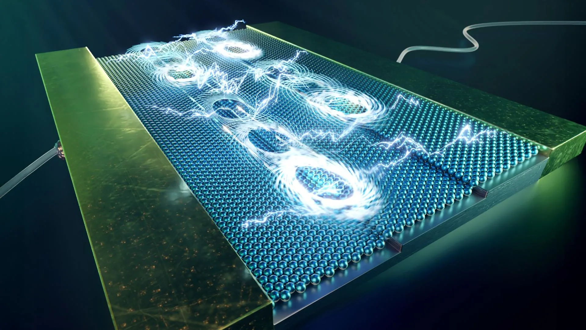
Physicists discovered on superconductor surfaces that single-atom steps just one atom high can guide the motion of quantum vortices, making vortex motion in a specific unidirectional path over 1,000 times easier than in the reverse direction[33]. Technically, this reveals a new physical mechanism at the atomic limit scale for applying strong asymmetric rectified guidance to flux vortex motion, providing an atomic-level directional control method to eliminate dissipation and decoherence caused by vortex creep in superconducting microwave cavities and qubit devices[33]. In terms of landscape impact, this opens a new avenue for superconducting qubit materials research to overcome two-level system (TLS) decoherence lifetime bottlenecks via microscopic material interface engineering[33].

Researchers at CIC nanoGUNE in Spain, in collaboration with the University of Santiago de Compostela, demonstrated that adding or removing a single molecule in a 1D quantum chain fundamentally alters the microscopic interaction between the entire molecular chain and the superconductor[8]. Technically, this validates for the first time at the atomic scale the ultra-sensitive control exerted by an individual building block in a molecular topological chain over superconducting proximity effects and bound-state energy levels, offering a highly controllable single-molecule switch for engineering molecular-scale spin quantum devices[8]. In terms of landscape impact, this provides the topological quantum computing and molecular spin physics communities with a more synthetically accessible organic molecular chemistry platform to explore topological physics such as Majorana zero modes[8].

QuTech in the Netherlands announced that it is leading and coordinating the Quantum Internet Alliance (QIA), bringing together top European industry, academic, and research entities to officially begin constructing the world's first full-stack quantum internet prototype system[32]. Technically, this surpasses the threshold of point-to-point physical interconnection experiments toward engineering system-level integration that spans underlying quantum memories, entanglement routing network layers, and high-level distributed application protocols[32]. In terms of landscape impact, this solidly cements Europe's global leadership position in establishing protocol standards for distributed quantum networks[32].

06Impact

Impacts Today

  1. Multinational Commercial Entities and Global Banking Settlement Networks (Target Audience: Foreign trade enterprises, cross-border clearing banks, and SWIFT network members): The WTO's official warning regarding a five-year cryptographic crack window[42] resonated with Germany's three-stage national mandatory PQC migration guideline spanning through 2035[15][40], signaling that post-quantum cryptography has officially spilled over from defense and intelligence spheres to become a statutory compliance deadline for multinational finance and commercial trade. Concurrently, the launch of commercial bank testnets[24] and response frameworks from mainstream digital asset platforms[4] established defensive postures. What to watch next: Certification outcomes of hybrid encryption algorithm standards across major foreign exchange clearing and settlement platforms prior to 2027, alongside quantum-resistant pilots for electronic bills of lading in cross-border trade.
  2. Fault-Tolerant Quantum Full-Stack Developers and Semiconductor Foundries (Target Audience: Superconducting and neutral-atom startups, silicon foundries, and EDA design tool vendors): The technical bottleneck of physical error-correction overhead is being rapidly closed in from both algorithmic and engineering fronts. Google's modular hyperbolic codes compress physical qubit requirements by over 30x[14], while MIT's ultra-compact code achieves a high-density encoding ratio better than 1:2[22]; coupled with Anderon's release of the first superconducting PDK on 300 mm wafers[18][39] and IBM's automated design workshop for dedicated decoding chips[16], the capital threshold and hardware lead times for fault-tolerant system development are dropping nonlinearly. What to watch next: On-hardware, small-scale integration validation of modular hyperbolic codes on physical superconducting chips or neutral-atom arrays, and the inaugural TLS defect density test reports for chips manufactured on Anderon's 300 mm foundry line.
  3. Telecommunications Infrastructure Operators and Compute Orchestration Platforms (Target Audience: Global major telecom backbone operators and datacenter infrastructure providers): The production-grade value of quantum annealing technology in hyperscale operations research and scheduling has been thoroughly validated. NTT DOCOMO's expansion of D-Wave solutions across its network of over 93 million mobile subscribers[28] proves that targeted annealing compute has closed the ROI loop in near-term commercial optimization scenarios. At the long-distance network tier, Europe initiated the construction of a full-stack quantum internet prototype[32], fiber-based MDI-QKD doubled its repeaterless key-generation distance beyond 300 km[30], and strong optoacoustic coupling in optical fibers endowed the transmission medium with in situ quantum processing capabilities[7]. What to watch next: The replication pace of D-Wave quantum annealing in larger-scale cross-border logistics and power grid dispatching, as well as commercial field test progress of long-distance QKD based on time-bin multiplexing.
  4. Cryptographic Security Hardware Vendors and Investment Institutions (Target Audience: Security chip manufacturers, PKI providers, and deep-tech venture capital): The post-quantum chip industry is shifting from early-stage R&D toward heavy capital expenditure expansion. SEALSQ confirmed $465 million in capital reserves dedicated to post-quantum semiconductors[21], and alongside the USPTO's tilt toward domestic manufacturing considerations[20], capital is accelerating into firms equipped with wafer fabrication and mature mass-production capabilities for hardware secure elements. What to watch next: Certification results for the initial commercial shipments of post-quantum ASIC chips from leading vendors like SEALSQ in Q4 2026, alongside US and European legislative movements on PQC compliance standards for imported electronic components.
07Other

Editorial Commentary

The technological evolution of fault-tolerant quantum computing is undergoing a profound paradigm shift—transitioning from brute-force physical qubit stacking to engineering refinement driven by error-correcting topological mathematics and standardized wafer fabrication. For years, the punishing overhead requiring hundreds of physical qubits for a single logical qubit was seen as the greatest hurdle hanging over universal fault-tolerant machines. Yet, newly emergent compact error-correcting codes and modular hyperbolic geometric architectures have theoretically slashed physical qubit overhead by more than an order of magnitude, even shattering traditional empirical lower bounds on physical-to-logical encoding ratios. Concurrently, the introduction of 300 mm standard semiconductor foundry kits and automated specialized chip design workshops marks quantum hardware's departure from the artisanal era of bespoke customization. This resonance between low-level algorithmic efficiency and mature semiconductor engineering capabilities is significantly pulling forward the realization timeline for commercial logical computing power.

On the industrial security and regulatory front, post-quantum cryptographic defenses have moved entirely past the boy-who-cried-wolf phase of alarmism into an operational stage driven by stringent regulations and concrete timelines. The coordinated schedules mapped out by international multilateral organizations and sovereign governments are crystal clear: this is not a distant concern reserved for post-2035, but a reconstruction of defensive perimeters with only a few years remaining on the clock. Capital market flows substantiate this reality—hundreds of millions of dollars in real capital are pouring into post-quantum semiconductor fabrication and real-world test sandboxes for financial-grade payment networks, rather than languishing in theoretical debate. For investors and technology decision-makers in this arena, breakthroughs in compute R&D and the reconstruction of information defenses are evolving symmetrically: whoever can first leap forward in low-redundancy error-corrected hardware, or secure a supply chain niche in the post-quantum chip replacement wave, will hold an unassailable position in the computational shifts of the coming decade.