Ion Traps: Fused-Silica Monolithic 3D Ion Trap Overcomes High-Voltage Confinement and Heating Bottlenecks for Heavy Ions
A joint research team from Rice University, Duke University, and Translume Inc. has developed a monolithic segmented three-dimensional ion trap based on fused-silica glass micromachining, publishing comprehensive physical measurement data in Physical Review Applied[2]. The chip-scale device can withstand radiofrequency (RF) drive voltages of several hundred volts, successfully achieving stable trapping of heavy ions such as ytterbium[2].
This advancement bridges a long-standing engineering gap between manually assembled macroscopic blade-type 3D traps and micromachined planar 2D chip traps[2]. While conventional hand-assembled macro blade traps feature deep potential wells and low radial motional heating rates (measured in phonon increments per second), their assembly tolerances exceed several micrometers and cannot be standardized for batch replication; conversely, standard semiconductor 2D surface traps offer micrometer precision but struggle to tolerate the ultra-high RF voltages required to drive heavy ions[2]. This monolithic 3D microstructure directly compresses electrode alignment tolerances to the sub-micron scale while effectively suppressing the ion heating rate[2].
Benchmarked against current ion-trap state-of-the-art (SOTA): in universal commercial systems, the highest recorded two-qubit gate fidelity across all qubit pairs on a chip is 99.921% on Quantinuum Helios (all-to-all connectivity across 98 barium-137 ions), while the best laboratory record for an isolated qubit pair reaches 99.99% on prototypes from Oxford Ionics and IonQ; this result advances the miniaturization and heavy-ion confinement capabilities of dedicated physical simulation platforms[2]. The critical missing elements standing between this milestone and fault-tolerant practical utility include severe electromagnetic crosstalk between RF electrodes during multi-physical-qubit scaling, as well as the ion transport heating overhead faced by quantum charge-coupled device (QCCD) multi-zone shuttling architectures, which still require validation of sympathetic cooling protocols and gate fidelity uniformity across long ion chains.
Because heavy ions such as ytterbium serve as core physical carriers for simulating photosynthetic charge transfer and complex molecular bond fission, the monolithic micromachining process eliminates the manual barriers of experimental system assembly. This allows high-precision photochemical quantum simulation experiments—previously confined to a handful of elite national laboratories—to expand into university laboratories, establishing an alternative foundational device manufacturing pathway that diversifies beyond full-stack ion-trap hardware startups[2].
Photonics & Solid-State Spins: Gallium Phosphide–Diamond Hybrid Photonic Chip Achieves Strong Interaction Coupling
A joint scientific team from the University of Washington and Pacific Northwest National Laboratory has developed a novel hybrid photonic integrated chip by directly integrating high-index gallium phosphide (GaP) nanophotonic microcavities onto diamond substrates hosting silicon-vacancy (SiV) centers (diamond point-defect qubits), with findings officially published in the international optical journal Optica Quantum[5]. Measurements demonstrated that the optical cooperativity between the microcavity optical mode field and a single SiV center (a key figure of merit for light-qubit interaction strength) surpassed the strong coupling threshold of 1 for the first time, while maintaining a spin coherence relaxation time exceeding 0.4 milliseconds in a 4 K cryostat environment[5].
By employing micro-stamp transfer printing, this approach circumvents the lattice damage caused by direct ion-beam etching of single-crystal diamond, achieving sub-micron photonic mode confinement while preserving the ultra-narrow optical emission linewidths of diamond color centers for the first time[5]. Conventional diamond microfabrication often induces lattice strain surrounding color centers, triggering random transition frequency shifts of hundreds of gigahertz; the high refractive index (approximately 3.3) and ultra-wide transparency window of gallium phosphide enable the creation of compact microcavities, boosting color-center resonance fluorescence collection efficiency to more than five times that of conventional bulk diamond[5].
Benchmarked against photonic quantum system SOTA: in pure photonic measurement-based platforms, PsiQuantum has demonstrated dual-rail encoded SPAM (state preparation and measurement) fidelities of 99.98% and two-qubit fusion fidelities of 99.22% on GlobalFoundries 300 mm production lines; this breakthrough serves as a crucial conversion interface between optical-fiber flying qubits and solid-state stationary qubits, advancing strong coupling interactions between solid-state spins and on-chip waveguides[5]. The critical missing elements before fault-tolerant networking can be realized include: current reported fidelities remain post-selected on detecting scattered photons; the chip lacks an end-to-end optical loss budget allocation; and butt-coupling insertion losses between on-chip nanowaveguides and single-mode telecom fibers still exceed 40%, leaving thermal mismatches and packaging mechanical drift urgently in need of resolution.
Affected stakeholders span research institutions and commercial enterprises developing distributed quantum computing interconnects and long-distance quantum repeaters. By coupling the exceptional telecom-band coherence of diamond color centers with standard semiconductor manufacturing compatibility via GaP processing, this work establishes an engineering roadmap for fabricating on-chip quantum routing and switching nodes within three years[5].
Solid-State Defect Mechanisms: Lattice Phonon Scattering Model Solves Spin Relaxation Puzzle in Diamond and Silicon Carbide
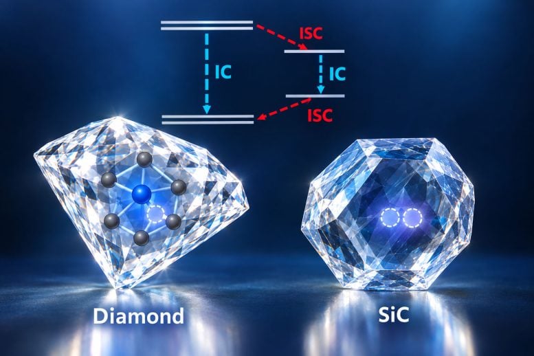
A research team at the Pritzker School of Molecular Engineering at the University of Chicago has constructed the first many-body computational physics model capable of accurately simulating the entire energy relaxation process of optically excited states in solid-state spin defects, uncovering the microscopic non-radiative decay mechanisms within nitrogen-vacancy (NV) centers in diamond and divacancy defects in silicon carbide (SiC)[13]. The model quantitatively reproduces, from first-principles calculations, the internal conversion process in which excited charges dissipate energy via lattice phonons (quanta of lattice vibrations), bringing theoretical luminescence lifetime predictions into agreement with experimental optical spectroscopy[13].
For decades, the development of quantum sensors and solid-state spin chips was hindered by a pronounced mismatch between theoretical lifetime predictions and observed spectra, primarily because prior algorithms could not quantify the non-radiative transition probability from spin-excited states into lattice mechanical vibrations[13]. By incorporating microscopic many-body electron-phonon interaction tensors into dynamical evolution simulations, the team identified the dominant role played by phonon dissipation channels, delivering a first-principles design tool for engineering defect configurations with extended coherence lifetimes[13].
This milestone will directly empower chip designers developing industrial-grade high-precision magnetometers, quantum gyroscopes, and spin memories on silicon carbide and diamond platforms, while enabling semiconductor material manufacturers to optimize impurity ratios and doping processes in epitaxial wafers based on these insights[13].
Topological Photonics: Programmable Photonic Chip Achieves First Real-Time Characterization of Topological Stability in Dissipative Systems
Researchers at the KTH Royal Institute of Technology in Sweden have developed a programmable integrated photonic chip architecture that, for the first time, directly measures topological invariants (parameters governing noise-resilient topological properties) that shield optical wave propagation from fabrication defect scattering within real-world dissipative optical devices[3]. Experimental results demonstrate that the system can dynamically reconfigure loss and coupling coefficients across an on-chip waveguide array on microsecond timescales, experimentally reconstructing a non-Hermitian (non-energy-conserving physical system) topological phase diagram[3].
Due to manufacturing imperfections, practical optical waveguides and optical fibers inevitably exhibit sidewall roughness and microscopic defects that cause severe photon scattering and phase distortion; topological photonic structures act like structural knots tied across waveguide arrays to prevent decoherence and scattering[3]. By dynamically tuning waveguide loss rates via an electro-optic modulator array, this chip circumvents the historical limitation of having to infer topological properties indirectly from idealized, lossless models, providing the first quantitative experimental calibration of topological anti-scattering robustness in a genuine chip environment[3].
Manufacturers of photonic quantum computing and fiber-optic sensing chips gain a testing platform for rapidly screening defect-resilient micro/nanophotonic waveguide designs, substantially trimming wafer tape-out trial-and-error cycles; this characterization methodology is anticipated to integrate into electronic-photonic design automation (EPDA) testing toolchains within two years[3].