Oct 25, 2026 – Oct 26 · Daily Brief

Quantum Simulation Tackles Fuel Cell Materials to Help Cut Costs for New Energy Vehicles

22 items · 7 sourcesPDFThis issue's roundup is free
02Hardware

Hardware Frontiers

Superconducting Architectures and Distributed Interconnects

IBM Watson Lab Develops 80 cm Coherent Interconnect Channel

A team at the IBM Thomas J. Watson Research Center successfully built an 80-centimeter coherent interconnect channel between superconducting quantum chips, achieving a 99% state transfer fidelity and advancing distributed controlled-Z gate (a fundamental two-qubit quantum logic gate, or CZ gate) fidelity to 96.42% ± 0.28%[5]. This milestone maintains high-fidelity inter-chip entanglement over a physical distance of nearly one meter; relative to the current superconducting single-chip SOTA baseline (median on-chip two-qubit gate fidelities of 99.5% to 99.9% in IBM Heron r2 and Google Willow), the current cross-chip CZ gate fidelity of 96.42% corresponds to an equivalent two-qubit error rate (approximately 3.58 × 10⁻²) that remains about an order of magnitude behind the on-chip baseline, yet successfully clears the physical spatial isolation threshold required for modular distributed scaling[5]. Reaching practical deployment still requires resolving cryogenic thermal load dissipation across dilution refrigerators for superconducting microwave links, as well as integrating microwave-to-optical coherent conversion modules[5]. This progress directly benefits full-stack vendors betting on modular multi-chip interconnects and is expected to reshape intra-cryostat chip layout standards within the next 2 to 3 years, reducing single-wafer area yield risks for thousand-qubit-scale superconducting processors[5].

Superconducting 12 ns CZ Gate Approaches Theoretical Limit

Researchers developed a superconducting CZ gate with an operation time of only 12 nanoseconds, approaching the theoretical quantum brachistochrone time limit of 11.6 nanoseconds while achieving intrinsic error suppression down to 2 × 10⁻⁵[6]. Experiments confirmed that even when high-frequency dephasing (random perturbations of quantum coherent states) in the device was increased to seven times existing measured baselines, the gate fidelity remained stable[6]. This metric compresses conventional superconducting two-qubit gate durations (typically 20 to 100 ns) by nearly half, while its theoretical intrinsic error of 2 × 10⁻⁵ effectively pushes fidelity to a 99.998% theoretical ceiling (claimed to surpass published SOTA levels, pending independent verification in multi-qubit arrays)[6]; practical fault-tolerant deployment still lacks empirical verification of parallel-drive crosstalk and leakage to higher energy states within dense multi-carrier-frequency arrays of hundreds of qubits[6]. This breakthrough will reduce the reliance of superconducting quantum chips on frequent calibrations during deep-circuit logical operations, accelerating the maturation of superconducting high-duty-cycle computing architectures[6].

ATS Coupler Achieves Ultra-High 9,922 Noise-Bias Ratio

A research team utilized an Asymmetrically Threaded SQUID (ATS) coupler to construct Kerr-cat bosonic qubit logic gates, achieving a noise-bias ratio of 9,922 (the ratio of phase-flip errors to bit-flip errors) under realistic photon loss rates—improving noise-biasing performance by over 570 times compared to conventional Kerr-cat implementations and attaining a two-qubit gate fidelity of 99.69%[7]. This metric clears the effective threshold for biased-noise fault-tolerant quantum error correction; the 99.69% two-qubit gate fidelity closely approaches the mainstream superconducting production SOTA range (99.5% to 99.9%), and its extreme noise bias allows 2D surface codes to focus primarily on correcting single-axis phase flips, reducing required physical qubit redundancy by several folds[7]; practical deployment, however, remains constrained by residual bit flips induced by multi-photon transition nonlinear dissipation and higher-order microwave channel losses[7]. This progress directly bolsters confidence among hardware startups focused on cat-state bosonic encoding, setting the stage over the next three years for more intense architectural competition between biased-noise error correction and conventional transmon approaches[7].

30 ns Quantum Gate Tolerates 4 MHz Parameter Drift

Researchers engineered a robust quantum gate with a 30-nanosecond gate duration that suppresses coupling error to 6.21 × 10⁻⁷ while tolerating inter-qubit interaction drift of up to 2π × 4 MHz[12]. Compared to conventional superconducting microwave pulse schemes requiring frequent calibration, this gate achieves dedicated error suppression within a standard 30 ns gate window, enabling hardware to passively resist coupling parameter fluctuations caused by environmental noise and thermal drift[12]; measured empirical data on spectral crowding during multi-qubit parallel execution are still lacking[12]. This technique benefits control and measurement system vendors by reducing the proportion of daily calibration time required by superconducting systems, thereby shortening offline maintenance windows for quantum cloud platforms[12].

Neutral-Atom Ecosystem and Systemic Bottlenecks

Assessment of China's Neutral-Atom Ecosystem Reveals System-Level Error-Correction Shortcomings

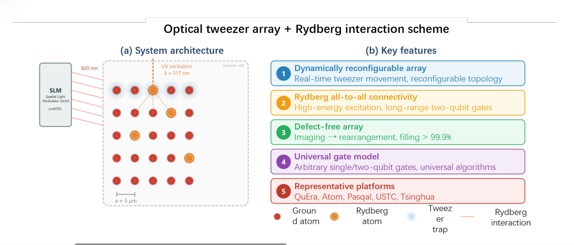
The latest review of China's neutral-atom quantum computing ecosystem indicates that domestic teams have achieved dense hardware milestones in optical tweezer trap array scaling, high-fidelity quantum gates, and commercial full-stack system integration, underpinned by an independent and complete optical and vacuum supply chain; however, they still lag behind European and US teams in system-level quantum error correction and fault-tolerant quantum computing[4]. In terms of physical qubit hardware metrics, domestic multi-thousand-atom trapping capabilities match or exceed Atom Computing's public baseline of 1,180 physical qubits and Harvard University's multi-thousand-atom arrays; yet regarding verified logical qubit metrics, compared to QuEra's demonstration of error-corrected gate operations across 96 logical qubits (based on [[16,6,4]] codes and 448 physical qubits, published in Nature 2026) and Quantinuum's 48 fully error-corrected logical qubits, domestic efforts face a generational gap of 1 to 2 years in real-time error-correction loops and transversal fault-tolerant logic gates[4]. The fundamental hard constraints holding this modality back from practical utility remain the single-cycle repetition rate (currently constrained by a low-frequency bottleneck of 1 to 10 Hz) and the fidelity of non-destructive mid-circuit measurements[4]. This assessment is prompting domestic industry-academia-research alliances to restructure R&D priorities, with capital and research resources expected to accelerate away from mere physical atom count accumulation toward logical qubit encoding and real-time FPGA decoder development over the next 12 months[4].

Solid-State Spins and Color-Center Defects

Germanium-Vacancy Color Center Conversion Efficiency in Diamond Reaches 90%

By introducing germane (GeH₄) during diamond chemical vapor deposition growth, researchers achieved targeted conversion of vacancies into germanium-vacancy (GeV⁻) color center defects within an ultra-thin 10-nanometer layer, reaching a defect conversion efficiency exceeding 90% while maintaining a spin coherence dephasing time (T₂) of over 730 nanoseconds[13]. This technique circumvents the inhomogeneous local lattice strain caused by traditional ion implantation, vaulting conversion efficiency from under 5% in conventional implantation to over 90%, with spin coherence times matching top-tier ion-implanted samples[13]; nevertheless, it still lags three orders of magnitude behind the millisecond-scale coherence baseline of NV centers, and its practical implementation remains reliant on sub-Kelvin cryogenic environments and efficient photon coupling via nanophotonic cavities[13]. This breakthrough provides a high-yield, scalable solid-state color-center material platform for distributed quantum network nodes and on-chip quantum memories, lowering manufacturing barriers for solid-state quantum repeaters[13].

University of Tsukuba Extends Coherence Time to 112 Seconds Using Polarized Spin Bath

A team from the University of Tsukuba in Japan, operating under a 25-Gauss magnetic field, utilized an optically polarized NV⁻ defect spin bath to maintain the spin coherence time of a ¹⁵NV⁻ sensor probe at 112 seconds (a 6.18-fold extension over the 18.1 seconds measured in a conventional P1 defect system of identical density); however, experiments also revealed that this advantage decays as the external magnetic field increases, vanishing entirely at 800 Gauss, where the polarized spin bath underperformed conventional substrates[18]. This experiment elucidates the physical mechanism by which polarized spin baths suppress many-body decoherence at low magnetic fields, advancing coherence lifetimes past the hundred-second threshold[18]; however, this performance reversal at high fields clearly limits the applicability of this method in high-field sensing scenarios such as nuclear magnetic resonance (NMR)[18]. This advance outlines a process optimization path for diamond quantum sensors in low-field, ultra-weak magnetic detection (such as magnetoencephalography and biological weak magnetic sensing), preventing misdirected engineering investments in high-field settings[18].

03Algorithms

Algorithms and Software

Modular Error Correction and Compilation Acceleration

Google and MIT Modular Design Cuts Error-Correction Overhead Tenfold

A joint Google-MIT team proposed a planar modular architecture using non-local inter-module interconnects that reduces physical qubit overhead by more than tenfold compared to conventional planar surface codes while achieving fault-tolerant quantum error correction[10]. Although operating below the error threshold in conventional planar surface codes has been demonstrated by Google Willow (error suppression factor Λ ≈ 2.1) and others, their physical-to-logical qubit encoding ratio typically reaches 105:1 or even over a thousand-to-one, requiring millions of physical qubits to run practical algorithms; this modular design breaks 2D locality constraints by introducing non-local inter-module connections, compressing the encoding ratio by an order of magnitude (approaching the high code rates of Quantinuum's 2:1 concatenated code and QuEra's ~4.7:1)[10]; the primary engineering hurdle lies in realizing high-fidelity inter-module quantum interconnect channels[10]. This achievement directly rewrites technical roadmaps for superconducting and silicon modalities constrained by planar 2D routing architectures, prompting global system vendors to re-evaluate chiplet stitching and multi-core on-chip interconnect compilation schemes, potentially advancing hardware delivery timelines by 2 to 3 years[10].

Hypergraph Algorithm Speeds Up Quantum Circuit Template Optimization by 606×

Researchers introduced a quantum circuit optimization framework based on hypergraph representations (topological network models composed of multi-node generalized hyperedges), boosting template matching optimization speed by up to 606 times compared to leading existing compilers such as IBM Qiskit[9]. The algorithm overcomes the theoretical bottleneck of local topological connectivity loss common in traditional simplification routines, fully preserving local circuit context while eliminating redundant matching computations and drastically cutting compilation time for deep circuits exceeding thousands of gates[9]. This approach directly benefits quantum cloud software stacks by compressing cloud pre-compilation latency for deep variational algorithms from hours to seconds, exerting performance replacement pressure on existing open-source compilation tools[9].

Lattice Surgery Dynamic Routing Saves 55.6% Space-Time Overhead

An R&D team developed an on-demand routing space architecture for lattice surgery compilation (geometric merging and splitting operations on topological quantum error-correcting codes), cutting space-time overhead (the physical resource product of spatial footprint and temporal cycles) by 55.6% during quantum algorithm execution, while accelerating compilation speed by 75.5 times compared to the leading tool DasCot[11]. This technique marks the first dynamic, elastic allocation of error-corrected logical qubit routing channels, eliminating the extensive physical qubit idling caused by statically reserved routing paths and directly boosting the comprehensive space-time utilization efficiency of fault-tolerant processors[11]. This architecture is poised to become a core candidate specification for fault-tolerant quantum compilers, helping execute more complex fault-tolerant logic gate sequences within constrained physical chip dimensions[11].

Simulation Algorithms and Many-Body Encodings

30-Qubit Variational Algorithm Achieves Relative Error of 10⁻⁵

Researchers developed a novel variational quantum algorithm tailored for complex particle physics simulations, achieving state preparation with under 1% error on a 30-qubit circuit, a relative variational energy error as low as 1 × 10⁻⁵, and extending numerical extrapolations to a 400-qubit scale[14]. The algorithm surpasses previous benchmarks in high-energy physics simulations, sustaining exceptionally low fitting deviations at the 400-qubit scale and breaking through the accuracy bottlenecks of classical approximation methods in strongly correlated quark systems[14]. This advance broadens the exploratory frontier for applying noisy intermediate-scale quantum hardware to high-energy and nuclear physics[14].

56-Qubit Chip Validates Advantages of Binary Orthogonal Encoding

A research team evaluated binary orthogonal encoding schemes on a 56-qubit superconducting processor to simulate discrete many-body bosonic systems, achieving a superior space-time trade-off between computational precision and quantum resource consumption compared to conventional direct discretization schemes[16]. Experiments confirmed that binary orthogonal encoding outperforms standard approaches in combined space (physical qubit count) and time (logical circuit depth) overhead, while noting that newly explored Dicke state encodings, despite extremely high execution speeds, require several times more physical qubit overhead[16]. These findings establish a standardized operator toolkit for continuous-variable discretization in quantum chemistry and condensed-matter physics simulations[16].

04Industry

Industry and Ecosystem

Government Capital Infusion and Semiconductor Foundry Manufacturing

New York State Finalizes Nearly $1.73B Quantum Industry Funding Package

The New York State Government announced the deployment of $360 million in dedicated funding for the quantum technology industry, with $300 million earmarked to establish a Quantum Research and Innovation Hub at Stony Brook University, $60 million directed to regional commercialization centers, and $1.37 billion secured in targeted matching funds from federal chip foundry initiatives[3]. This marks the formation of a nearly $1.73 billion public-private-academic consortium that shifts the industrial model from early, fragmented university laboratory incubation toward scaled industrial clusters anchored by 300 mm wafer foundry capabilities—directly closing the industrial loop from superconducting, photonic, and silicon quantum device tape-outs to enterprise compute demands[3]. This investment solidifies the US East Coast's position as a quantum hardware manufacturing cluster, directly benefiting regional semiconductor and quantum assets, and is projected to generate over a thousand advanced manufacturing jobs within the next 3 to 5 years[3].

New Mexico Allocates Over $12M to Fund Hardware Talent Expansion

Under its FY2022 Q1 Job Training Incentive Program (JTIP), the New Mexico State Government allocated over $12 million to subsidize publicly traded trapped-ion quantum computing firm IonQ and Bandelier Technologies, specifically supporting workforce expansion in hardware engineering, quantum systems operations and maintenance, quantum lidar, quantum sensing, and metasurface communications R&D[2]. Direct government subsidies help offset the steep early labor costs of hands-on engineering technicians and systems maintenance personnel for deep-tech companies, signaling that trapped-ion hardware manufacturing has entered a phase of scaled expansion characterized by standardized assembly and equipment maintenance[2]. This funding secures capital for the trapped-ion modality to establish a second manufacturing base in the United States, optimizing cash flow for manufacturing-oriented enterprises and accelerating the localized training of non-academic practical technical workers[2].

Capital Cycles and Transnational Standards

Capital Markets Set 2028 Commercial Reality Check for Quantum Stocks

A late October 2026 assessment report from tech industry think tanks and mainstream financial media analyzing publicly traded quantum computing companies indicates that secondary-market quantum stocks will face a pivotal commercial reality check in 2028, when capital markets will reassess valuations based on realized commercial contract revenue and fault-tolerant system delivery progress[1]. This marks an end to valuation models fueled purely by conceptual narratives and modest early R&D cloud-access fees; investment institutions are shifting fully toward due diligence criteria centered on gross margins, genuine commercial compute orders, and fault-tolerant logical qubit delivery milestones[1]. Compressing secondary-market valuation multiples will force public companies to rein in cash burn rates before 2028, while accelerating the concentration of primary market capital into top-tier startups possessing tangible industrial deployment capabilities[1].

Benelux-QCI Partners Advance European Quantum Secure Communication Backbone

On October 22, 2026, Quantum Delta NL (QDNL) hosted the Benelux Quantum Communication Infrastructure (Benelux-QCI) partner meeting in Utrecht, where representatives from the Netherlands, Belgium, Luxembourg, and Greece established four priority action tracks to advance cross-border quantum key distribution (QKD) under the European Quantum Communication Infrastructure (EuroQCI): capability building, end-user validation, cross-border demonstrations, and international standards development[22]. This marks a transition for Europe's state-led sovereign encrypted communications network from single-nation intranet trials into a phase of cross-border backbone protocol interoperability and interface standardization[22]. The initiative creates clear procurement tender windows for European native QKD hardware vendors and telecom operators, accelerating the unification of cross-border power-grid quantum communication protocols and financial encryption interface standards[22].

05Other

Academic Frontiers

Cross-Disciplinary Industrial Computing and High-Precision Frequency Standards

Quantum Workflow Directly Bridges Fuel Cell Electrode Economic Assessment

Researchers developed an end-to-end quantum simulation workflow for screening fuel cell materials, employing Green's functions combined with dynamical mean-field theory (GW+DMFT) and self-energy embedding theory (SEET) to simulate the atomic-scale interface characteristics of strongly correlated oxygen reduction reaction (ORR) electrodes and link them directly to economic cost-benefit models for operational fuel cells[8]. This approach bridges the multi-tier approximation gap between atomic-scale quantum many-body physics simulations and macroscopic engineering economics for the first time, eliminating past predictive errors in electrode lifespan and reaction barriers caused by empirical parameters, and demonstrating the end-to-end capability of quantum computing to move from fundamental material physics to real-world industrial cost assessments[8]. This breakthrough directly benefits clean-energy automotive OEMs, fuel cell stack manufacturers, and hydrogen materials laboratories, cutting screening cycles for precious-metal-free catalyst alternatives from years to months[8].

Transnational Atomic Clock Comparison Precision Surpasses 5 × 10⁻¹⁸ for the First Time

An international metrology research team completed a high-precision atomic clock comparison experiment across a 2,220-kilometer physical optical fiber network, achieving a time-frequency measurement precision better than 5 × 10⁻¹⁸ on a transnational scale for the first time and tightening the physical upper bound on potential temporal drift of the fine-structure constant (α) by a factor of five[15]. This achievement sets an all-time record for precision in long-range transnational optical frequency standard comparisons, directly clearing the technical threshold set by the International Committee for Weights and Measures (CIPM) to redefine the SI second, making the wholesale replacement of traditional microwave cesium atomic clocks by next-generation optical transition frequency standards a foregone conclusion[15]. This technology will fundamentally reshape global distributed time synchronization infrastructure, serving as a critical pillar for satellite navigation, microsecond-level fault isolation in global power grids, and very-long-baseline interferometry (VLBI) in radio astronomy[15].

Matter-Wave Spin Squeezing Sets New Record at -14.57 dB

An experimental team demonstrated -14.57 dB of spin squeezing (a quantum-correlation enhancement technique that beats the standard shot-noise limit) in a matter-wave quantum sensing system, breaking previous physical records held by oscillation control schemes (-10 dB) and Bose-Einstein condensate (BEC) interferometers (-7.8 ± 0.8 dB)[17]. This advance nearly doubles the margin by which matter-wave interferometers surpass the standard quantum limit (suppressing noise by more than 4.57 dB), establishing an ultra-low-noise front end for atomic gravimeters, gravity gradiometers, and high-sensitivity inertial navigation systems[17]. This benefits the instrumentation of quantum precision measurement devices and the development of autonomous, GPS-denied navigation systems for deep-sea and subterranean environments[17].

Single-Atom Defect Imaging Unveils Electron-Wave Interference in Unconventional Metals

Using scanning tunneling microscopy (STM) to probe single-atom defects inside unconventional metallic materials, condensed matter physicists captured distinctive quantum interference scattering patterns of conduction electron waves, revealing non-trivial transport behavior protected by topological physics within the metal[20]. This experiment provides direct, real-space atomic-scale observational evidence of the Fermi surface topology in strongly correlated unconventional conductors, circumventing the limitations of macroscopic averaged measurements that wash out local electronic interactions[20]. These findings offer fundamental experimental guidance for exploring mechanisms behind novel low-dissipation quantum electronic devices and unconventional superconducting materials[20].

06Other

Today's Implications

  1. Major Semiconductor Foundries and Superconducting Quantum Hardware Vendors: New York State's joint $1.73 billion initiative with the federal government to establish a foundry hub, combined with Google and MIT's modular architecture slashing error-correction physical qubit overhead tenfold, signals that quantum computing is moving away from the single-chip limit era toward standardized mass production reliant on 300 mm foundries and modular multi-chip interconnects[3][10]. The next focus is monitoring quantum process yield ramps at foundries like GlobalFoundries and the formulation of microwave-to-optical interconnect standards.
  2. Clean-Energy Automakers and Fuel Cell Electrode R&D Teams: Quantum algorithms have for the first time unified the modeling pipeline from microscopic interface physics in strongly correlated oxygen electrodes to macroscopic battery economics, eliminating empirical approximations and drastically shortening screening iterations for non-precious-metal catalysts[8]. The next focus is tracking collaborative algorithm validation between automotive materials labs and quantum software teams using operational stack data.
  3. Neutral-Atom Quantum Computing R&D Ecosystem: Global industry assessment criteria for neutral-atom systems have shifted decisively from optical tweezer atom counts to the ability to execute high-repetition-rate error correction and transversal logic gates; while Chinese hardware maintains scale advantages in physical arrays and upstream supply chains, generational lags in logical qubit error correction are forcing domestic teams to reorder R&D priorities[4]. The next focus is monitoring breakthroughs by leading domestic research institutions in real-time decoder ASICs/FPGAs and continuous-loading architectures.
  4. Precision Navigation and Time-Frequency Metrology Supply Chains: Transnational atomic clock comparisons have cleared the 5 × 10⁻¹⁸ precision threshold, laying the final cornerstone for the optical redefinition of the SI second, while matter-wave spin squeezing reached a record -14.57 dB[15][17]. The next focus is the engineering transition of fiber-optic time-transfer networks and transportable optical frequency standards into next-generation centimeter-level ground stations for satellite navigation.
  5. Secondary-Market Quantum Tech Investors: With less than two years remaining before the 2028 commercial reality check, and regional subsidies in states like New Mexico tilting heavily toward hands-on technical personnel, relying solely on physical qubit counts will no longer sustain high valuation multiples[1][2]. The next focus is closely tracking fulfillment rates on commercial contracts and cash-burn risks among leading public companies.
07Other

Editorial Commentary

Hardware systems engineering is abandoning the "single-chip physical qubit arms race" in favor of "architectural co-optimization centered on error-correction overhead." From modular topologies with non-local interconnects cutting physical qubit overhead tenfold, to superconducting inter-chip microwave links achieving 99% state transfer fidelity, to compilers dynamically shrinking lattice surgery routing space, the industry is coalescing around a consensus: hardware scaling that fails to reduce physical redundancy offers no commercial viability. The current migration of capital from conceptual R&D into semiconductor foundry buildouts directly reflects this return to engineering pragmatism.

The valuation anchor for application deployment is narrowing from "generalized compute narratives" to "high-value industrial verticals." Whether directly quantifying financial returns through fuel cell electrode simulations or approaching the redefinition of time standards via transnational ultra-precise optical clock comparisons, quantum technology is undergoing rigorous real-world ROI scrutiny. Facing the 2028 commercialization reckoning in secondary markets, only architectures that compress physical error-correction overhead by orders of magnitude—while demonstrating irreplaceable precision in targeted industrial R&D workflows—will survive this capital cycle.