Superconducting Hardware: Millikelvin Cryogenic Control Power Plummets to Picowatt Levels
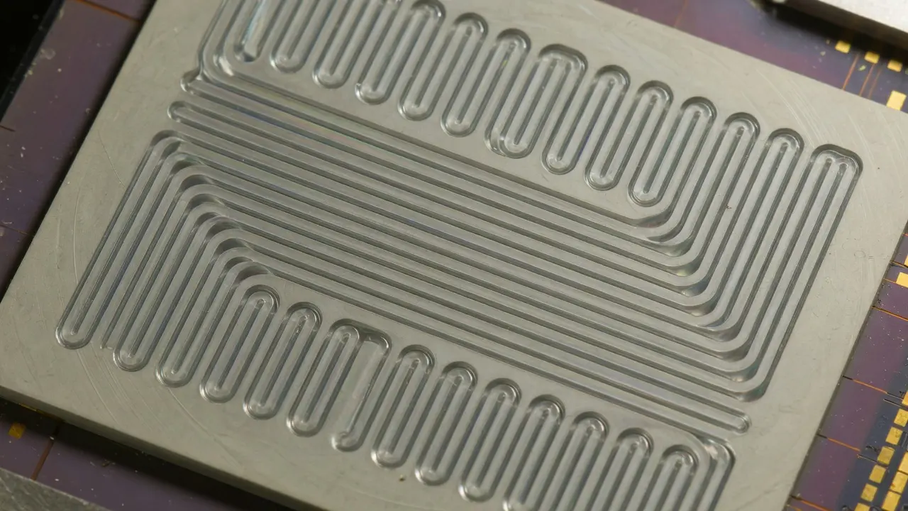
Publishing in Nature npj Quantum Information, an international research team demonstrated a cryo-CMOS RF multiplexer operating at millikelvin temperatures that achieves ultra-low static power dissipation at the picowatt level during superconducting qubit control, readout, and flux bias tasks [1].
From a technological advancement perspective, conventional cryogenic control chips operating at 3 to 4 Kelvin typically dissipate microwatts to milliwatts of power and cannot be placed directly into a millikelvin mixing chamber whose cooling capacity is merely several microwatts. This achievement suppresses control-line thermal dissipation to the picowatt level for the first time—a 3 to 6 order-of-magnitude reduction compared to traditional cryo-CMOS designs—pioneering direct-connected multiplexing at millikelvin temperatures [1]. Benchmarked against current state-of-the-art (SOTA) superconducting systems—Google Willow (105 physical qubits, median two-qubit gate fidelity of 99.7%) and IBM Nighthawk (120 physical qubits, 218 tunable couplers)—this chip has yet to complete empirical microwave pulse crosstalk and signal-to-noise ratio measurements on active, 100-qubit-scale quantum processors; furthermore, long-term DC flux drift and coherence fluctuations induced by two-level systems (energy-loss defects in materials) remain key bottlenecks constraining its progression toward industrial-grade integration [1].
From an industry landscape perspective, this breakthrough directly relieves the thermal loads and spatial congestion imposed by thousands of coaxial RF cables inside dilution refrigerators. This enables major hardware developers pursuing 10,000-qubit superconducting scaling to reduce underlying wiring complexity by at least an order of magnitude within the next 3 to 5 years, removing physical scaling roadblocks as superconducting platforms transition toward fault tolerance [1].
Solid-State Spin: 3D Tomography Unlocks Exchange Interactions, Spin-State Memories Chart New Pathways
Researchers have developed a three-dimensional tomography technique to map the accumulated exchange phase $\phi(V)$ of spin quantum dots as gate voltages vary continuously, overcoming a central hurdle in precisely extracting exchange interactions (quantum coupling between two electron spins) between quantum dots [21].
This technique elevates the characterization precision of spin qubit coupling strength to sub-millivolt resolution, thoroughly overturning previous calibration workflows that relied on trial-and-error and indirect measurements [21]. Compared to current SOTA benchmarks in spin architectures—where Australia's SQC has achieved 99.99% two-qubit gate fidelity with atomic-precision donor qubits, and Diraq has measured two-qubit gate fidelity exceeding 99% on mass-produced 300 mm wafer devices—current quantum dot processors generally remain limited to 12 physical qubits or fewer. While this tomography technique substantially accelerates two-qubit gate calibrations, it has not yet achieved automated parallel integration across 2D arrays containing thousands of quantum dots (such as the 1,024-quantum-dot array characterized by Quantum Motion), and cryogenic on-chip readout circuit bandwidth continues to constrain real-time deployment in large-scale arrays [21]. Spin-chip design startups are poised to adopt this high-precision phase-imaging tool over the next 1 to 2 years, accelerating the transition of silicon spin chips from laboratory prototypes to standardized foundry design libraries [21].
In quantum memory, physicists validated a high-performance telecom-band quantum memory based on electron spin states, which theoretically reduces physical qubit requirements in long-distance quantum communications and distributed networks to one-hundredth of previous levels [20]. Operating in the telecom C-band fiber window, the device demonstrated high-fidelity storage and on-demand retrieval of long-lived electron spin-photon entangled states for the first time, boosting the buffer efficiency of single-node quantum repeaters by nearly two orders of magnitude [20]. Against SOTA benchmarks for fiber-optic quantum interconnects (such as PsiQuantum's 99.72% inter-chip fiber interconnect fidelity), the end-to-end optical write/read conversion efficiency and polarization decoherence times of this spin memory still face engineering barriers, requiring several years of fabrication maturation before deployment across wide-area, low-loss repeater backbones [20]. This breakthrough lowers capital expenditure expectations for network providers focusing on quantum entanglement distribution and distributed interconnects, providing a new physical path toward long-haul backbone nodes [20].
Photonic Hardware: Routing Phase Shifters Halved, 100-km Optical Comb Synchronization Enters the Femtosecond Regime
An optical integration research team successfully constructed a $3 \times 3$ photonic router that uses $\mathcal{O}(N)$ programmable phase shifters to route signals between arbitrary input and output ports in exactly $N$ steps. This halves the active component complexity of conventional optical crossbar arrays or Mach-Zehnder interferometer meshes while achieving an extinction ratio exceeding 11 dB across target telecom bands [10].
The architecture bypasses the cumbersome fully connected matrix structures of conventional universal transformations, reducing the count of active control units by 50% while maintaining non-blocking signal switching [10]. Relative to photonic quantum computing SOTA baselines (e.g., PsiQuantum's Omega architecture, which relies on highly integrated barium titanate electro-optic switches to achieve a fusion gate fidelity of 99.22%), the primary hard constraint of photonic chips is the insertion loss introduced by each phase shifter and splitter. Halving the number of phase shifters directly cuts accumulated path loss; however, an end-to-end optical loss budget (accounting for waveguide losses, fiber-coupling losses, and superconducting nanowire single-photon detector efficiencies) remains to be established, and dynamic crosstalk must still be verified in measurement-based error-correcting systems incorporating non-classical entangled photon sources [10]. This streamlined routing approach will directly benefit photonic quantum hardware startups and optical interconnect module vendors, with projections to reduce chip manufacturing costs and power consumption in data centers and quantum optical switching matrices by approximately 40% within the next 2 to 3 years [10].
Leveraging optical frequency comb infrastructure, researchers achieved a clock stability of 0.85 femtoseconds (1 femtosecond = $10^{-15}$ seconds) over a 100 km commercial telecom fiber link, setting a new benchmark for time synchronization precision across long-haul quantum networks [14]. This marks the first time that bidirectional long-distance time synchronization jitter has been suppressed below 1 femtosecond—an improvement of more than $5\times$ over existing microwave optoelectronic conversion schemes—providing a foundational reference clock for frequency- and phase-locked distributed quantum computing nodes across cities [14]. Compared to existing quantum network interconnect trials, this frequency comb link exhibits exceptional phase stability; however, closed-loop automated polarization and dispersion compensation capabilities must still be proven in harsh field fiber environments subject to severe temperature fluctuations and ground vibrations [14]. The technique establishes a physical clock foundation for collaborative computation across regional distributed superconducting quantum clusters and is expected to be deployed first in national quantum secure communications backbones and high-precision deep-space ground stations [14].
In quantum sensing materials, a research team fabricated high-brightness, high-uniformity silicon carbide nanopillar arrays, setting a new record for photon count rates in scalable quantum sensors based on color-center defects [11]. The structure significantly enhances the fluorescence collection efficiency of individual spin color centers, pushing weak magnetic field and temperature sensing sensitivities to new highs and eliminating photon collection bottlenecks for on-chip integration in in vivo biological imaging and non-destructive inspection of micro-regions in semiconductor devices [11].